


 |
0.5mm LiNbO3 Substrate With TTV<5um Surface Roughness Ra<0.5nm
Product Details:
| Place of Origin: | China |
| Brand Name: | BonTek |
| Certification: | ISO:9001 |
| Model Number: | LiNbO3 |
Payment & Shipping Terms:
| Minimum Order Quantity: | 5 pcs |
|---|---|
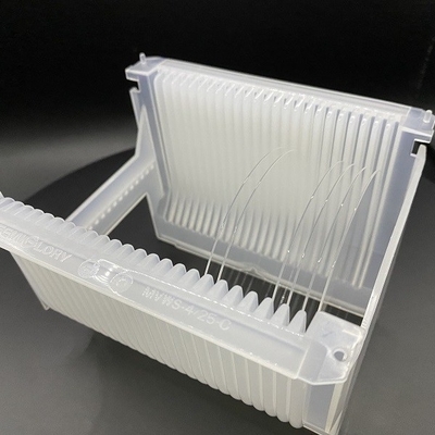
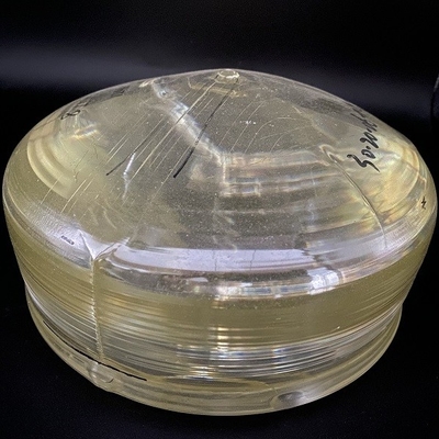
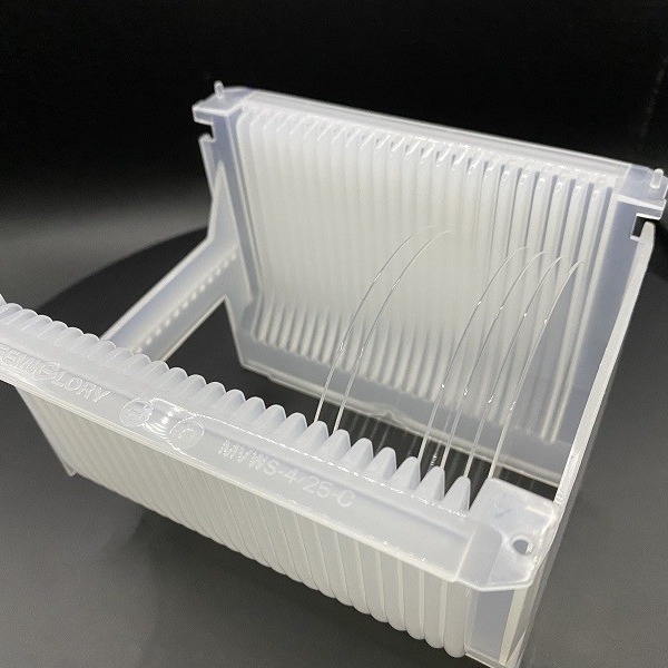
| Packaging Details: | Cassette, Jar |
| Delivery Time: | 2 weeks |
| Payment Terms: | TT/AD |
| Supply Ability: | 10000+ pcs/Month |
|
Detail Information |
|||
| Material: | LiNbO3 | Shape: | Round Wafer |
|---|---|---|---|
| Diameter: | 100mm, 150mm, 200mm | Thickness: | 0.5mm |
| TTV: | <5um | Bow: | <20um |
| Warp: | <40um | Edge Quality: | Beveled |
| Surface: | Polished | Surface Roughness: | Ra<0.5nm |
| Chips: | None | Test Report: | Available |
| Highlight: | 0.5mm LiNbO3 Substrate,LiNbO3 Substrate with TTV,Round LiNbO3 Wafer 200mm |
||
Product Description
Unlocking Infinite Possibilities with Lithium Niobate Wafers
Product Description:
Exceptional Quality Lithium Niobate Wafers for Your Cutting-Edge Applications
When innovation meets precision, you'll find Lithium Niobate Wafers - the foundation of countless technological breakthroughs. Our Lithium Niobate Wafers are designed to elevate your projects, delivering unparalleled performance and reliability. Explore the limitless potential of these wafers through their remarkable properties.
Features:
- Crystal Clarity for Unmatched Precision
Crafted with the utmost precision, our Lithium Niobate Wafers boast a crystal-clear structure that enhances the accuracy of your optical devices. Whether you're delving into photonics, telecommunications, or integrated optics, our wafers ensure minimal signal loss and maximum data fidelity, making your endeavors shine with brilliance.
- Robust and Versatile for Every Application
From acoustic wave devices to optical modulators, our Lithium Niobate Wafers adapt seamlessly to diverse applications. Their exceptional piezoelectric and electro-optic properties empower you to conquer the challenges of your projects, enabling you to push boundaries and explore new horizons in technology.
Technical Parameters:
| Diameter | 76.2±0.2mm | 100±0.2mm | 150±0.2mm | 200±0.2mm |
| Primary Flat | 22±1mm | 32±1mm | 47.5mm, 57.5mm, Notch | 57.5mm, Notch |
| Orientation | 36°Y, 42°Y, X-112°Y, Y, Z | |||
| Thickness | 0.07mm~5.0mm | 0.1mm~5.0mm | 0.35mm~5.0mm | 0.35mm~5.0mm |
| Surface finish | Single / Double side polish / Double side lapped | |||
| TTV | < 1~5µm | |||
| BOW | ± (20µm ~40um ) | |||
| Warp | <= 20µm ~ 50µm | |||
| LTV (5mmx5mm) | <1.5 um | |||
| PLTV(<0.5um) | ≥98% (5mm*5mm) with 2mm edge excluded | |||
| Polished side Ra | Roughness Ra<=5A | |||
| Back Side Criteria | Roughness Ra:0.5-1.0µm, GC#1000 | |||
| Scratch & Dig (S/D) | 20/10, 40/20, 60/40 | |||
| Edge Profile | Compl't with SEMI M1.2@with GC800# .regular at C typed | |||
| Cracks, saw marks, stains | None | |||
Applications:
BonTek's LiNbO3 wafer is a high-quality substrate used in a wide range of applications. The Lithium-Niobium-Wafer, also known as Lithium-Niobate-Wafer, is fabricated with a X-cut orientation and a BOW of less than 20um. It also features an incredibly smooth surface with a Ra value of 0.5nm. BonTek's LiNbO3 wafer is available in three different sizes: 100mm, 150mm, and 200mm. All of our products are certified with ISO:9001 and can be purchased in a minimum order quantity of 5 pcs. We can provide a delivery time of 2 weeks and accept payment terms of TT/AD. Our production capacity is 10,000+ pcs/Month.
BonTek's LiNbO3 wafer is widely used in various industries such as laser, telecom, and optics. It is a great choice for applications that require high stability, low optical loss, and excellent temperature and wavelength stability. It is also suitable for electro-optic modulator, optical isolator, optical modulator, lithium-niobate waveguide, and other optical components.
The LiNbO3 wafer from BonTek has the highest quality and offers unbeatable performance. All our products are packaged in a secure cassette or jar and are ready for shipment. With our advanced manufacturing technology and strict quality control, you can trust that you’ll be getting the best LiNbO3 wafers on the market.
Support and Services:
We provide technical support and services for LiNbO3 Wafer. Our services include:
- Assistance in selection of LiNbO3 Wafer for specific applications.
- Providing technical specifications for LiNbO3 Wafer.
- Assistance in installing and setting up the LiNbO3 Wafer.
- Providing training and educational materials to help users understand and use the LiNbO3 Wafer.
- Providing customer service, including answering questions, solving problems, and providing technical advice.
We strive to offer the highest quality of technical support and services for LiNbO3 Wafer.
Packing and Shipping:
The LiNbO3 wafer should be packaged and shipped carefully. Before packaging, it is necessary to check the quality and cleanliness of the wafer.
The packaging material should be clean and free from dust. The wafer should be placed in the middle of the package and surrounded by shock absorbing materials. The package should be sealed securely with tape.
During shipping, the package should be sealed tightly and handled carefully. The package should be labeled clearly to identify the content and ensure proper shipping.
Finally, the package should be inspected carefully before shipping to ensure that it is in good condition and ready for delivery.