


 |
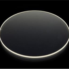
R-plane 1102 C-plane 0001 Sapphire Wafer For IR and UV Wavelength Applications
Product Details:
| Place of Origin: | China |
| Brand Name: | BonTek |
| Certification: | ISO:9001 |
| Model Number: | Sapphire (Al2O3) |
Payment & Shipping Terms:
| Minimum Order Quantity: | 5 Pieces |
|---|---|
| Price: | Negotiable |
| Packaging Details: | Cassette, Jar, Film package |
| Delivery Time: | 1-4 weeks |
| Payment Terms: | T/T |
| Supply Ability: | 10000 pieces/Month |
|
Detail Information |
|||
| Material: | Sapphire Wafer | Growth: | Kyropoulos Method |
|---|---|---|---|
| Melting Point: | 2040 Degrees C | Thermal Conductivity: | 27.21 W/(m X K) At 300 K |
| Thermal Expansion: | 5.6 X 10 -6 /K (parallel C-axis) & 5.0 (perpendicular C-axis) X 10 -6 /K | Hardness: | Knoop 2000 Kg/mm 2 With 2000g Indenter |
| Specific Heat Capacity: | 419 J/(kg X K) | Dielectric Constant: | 11.5 (parallel C-axis) 9.4 (perpendicular C-axis) At 1MHz |
| Highlight: | C-plane 0001 Sapphire Wafer,Kyropoulos single crystal sapphire,R-plane 1102 Sapphire Wafer |
||
Product Description
R-plane 1102 C-plane 0001 Sapphire Wafer For IR and UV Wavelength Applications
The growth method refers to the process by which the ingot of single crystal sapphire is produced. For most sapphire wafers this is the Kyropoulos method (abbreviated to Ky or Kr). The Kyropoulos method is a continuation of the Czochralski method (CZ) which is used in the manufacture of silicon wafers. The Kr method allows for the production of very large ingots of single crystal sapphire that can then be processed into wafers.
Typical cuts of sapphire are R-plane (1102), C-Plane (0001), A-plane (1120), M-plane (1010) and N-plane (1123). Orientation affects the physical properties of the sapphire wafers – and in particular how it integrates and lattice matches with other materials.
![]()
![]()
![]()
| OPTICAL PROPERTIES of SAPPHIRE Al2O3 | |
|
Transmission Range |
0.17 to 5.5 microns |
|
Refractive Index |
1.75449 (o) 1.74663 (e) at 1.06 microns |
|
Reflection Loss |
at 1.06 microns (2 surfaces) for o-ray - 11.7%; for e-ray - 14.2% |
|
Index of Absorption |
0.3 x 10⁻³ cm-1 at 2.4 microns |
|
dN/dT |
13.7 x 10⁻⁶ at 5.4 microns |
|
dn/dm = 0 |
1.5 microns |
| PHYSICAL PROPERTIES of SAPPHIRE Al2O3 | |
|
Density |
3.97 g/cm3 |
|
Melting Point |
2040 degrees C |
|
Thermal Conductivity |
27.21 W/(m x K) at 300 K |
|
Thermal Expansion |
5.6 x 10 -6 /K (parallel C-axis) & 5.0 (perpendicular C-axis) x 10 -6 /K |
|
Hardness |
Knoop 2000 kg/mm 2 with 2000g indenter |
|
Specific Heat Capacity |
419 J/(kg x K) |
|
Dielectric Constant |
11.5 (parallel C-axis) 9.4 (perpendicular C-axis) at 1MHz |
|
Young's Modulus (E) |
335 GPa |
|
Shear Modulus (G) |
148.1 GPa |
|
Bulk Modulus (K) |
240 GPa |
|
Elastic Coefficients |
C11=496 C12=164 C13=115 |
|
Apparent Elastic Limit |
275 MPa (40,000 psi) |
|
Poisson Ratio |
0.25 |
|
Orientation |
R-plane, C-plane, A-plane, M-plane or a specified orientation |
|
Orientation Tolerance |
± 0.3° |
|
Diameter |
2 inches, 3 inches, 4 inches, 6 inches, 8 inches or others |
|
Diameter Tolerance |
0.1mm for 2 inches, 0.2mm for 3 inches, 0.3mm for 4 inches, 0.5mm for 6 inches |
|
Thickness |
0.25mm, 0.33mm, 0.43mm, 0.65mm, 1mm or others; |
|
Thickness Tolerance |
25μm |
|
Primary Flat Length |
16.0±1.0mm for 2 inches, 22.0±1.0mm for 3 inches, 30.0±1.5mm for 4 inches, 47.5/50.0±2.0mm for 6 inches |
|
Primary Flat Orientation |
A-plane (1 1-2 0 ) ± 0.2°; C-plane (0 0-0 1 ) ± 0.2°, Projected C-Axis 45 +/- 2° |
|
TTV |
≤10µm for 2 inches, ≤15µm for 3 inches, ≤20µm for 4 inches, ≤25µm for 6 inches |
|
BOW |
≤10µm for 2 inches, ≤15µm for 3 inches, ≤20µm for 4 inches, ≤25µm for 6 inches |
|
Front Surface |
Epi-Polished (Ra< 0.3nm for C-plane, 0.5nm for other orientations) |
|
Back Surface |
Fine ground (Ra=0.6μm~1.4μm) or Epi-polished |
|
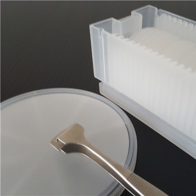
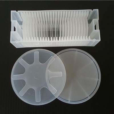
Packaging |
Packaged in a class 100 clean room environment |
![]()
Acceptance Check
![]()
1. The product is fragile. We have adequately packed it and labeled it fragile. We deliver through excellent domestic and international express companies to ensure transportation quality.
2. After receiving the goods, please handle with care and check whether the outer carton is in good condition. Carefully open the outer carton and check whether the packing boxes are in alignment. Take a picture before you take them out.
3. Please open the vacuum package in a clean room when the products are to be applied.
4. If the products are found damaged during courier, please take a picture or record a video immediately. DO NOT take the damaged products out of the packaging box! Contact us immediately and we will solve the problem well.