


 |
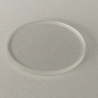
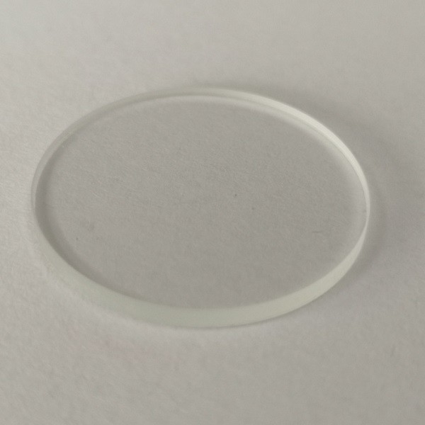
6 Inch 0.5mm Borofloat 33 Glass Substrate For Semiconductor Industry And MEMS
Product Details:
| Place of Origin: | China |
| Brand Name: | BonTek |
| Certification: | ISO:9001, ISO:14001 |
| Model Number: | Fused Silica, Fused Quartz |
Payment & Shipping Terms:
| Minimum Order Quantity: | 5 pcs |
|---|---|
| Price: | Negotiable |
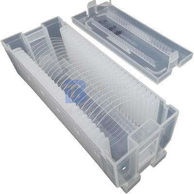
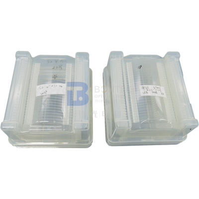
| Packaging Details: | Cassette/ Jar package, vaccum sealed |
| Delivery Time: | 1-4 weeks |
| Payment Terms: | T/T |
| Supply Ability: | 20000 pcs/Month |
|
Detail Information |
|||
| Material: | Borofloat 33 Glass Substrate | Type: | Borosilicate |
|---|---|---|---|
| Brand: | Schott Brorofloat 33 | Use: | Semiconductor, MEMS |
| Diameter: | 150mm | Thickness: | 0.5mm |
| Edge: | Ground C-shape | Surface Finish: | Single / Double Side Polish |
| Highlight: | 0.5mm Glass Substrate,Semiconductor Industry MEMS Substrate,6 inch Glass Substrate |
||
Product Description
6 inch 0.5mm Borofloat 33 Glass Substrate for Semiconductor Industry and MEMS
With its unique physical and chemical properties, BOROFLOAT33 has become a veritable multi-purpose :· Home appliances (doors, microwave glass, fireplace glass panels). Environmental engineering, chemical industry, lining of reaction kettle, fluid systems, corrosion resistance and observation of casting, lighting (spotlight and high-power floodlight protection panel), photovoltaic systems (solar cell coating substrate), precision engineering, optical (filters and mirrors, etc.), medical technology, biological technology (slides, biochip, titration, DNA array) semiconductor industry The quality of BOROFLOAT33 glass meets the requirements of DIN ISO 9001 and Schott's certification system.
![]()
![]()
![]()
|
Product |
BOROFLOAT 33 |
|
Density |
2.23 g/cm3 |
|
Modulus of Elasticity |
63 kN/mm2 |
|
Knoop Hardness HK 0.1/20 |
480 |
|
Poisson’s Ratio |
0.2 |
|
Dielectric Constant (@ 1 MHz & 25°C) |
4.6 |
|
Loss Tangent (@ 1 MHz & 25°C) |
37 x 10-4 |
|
Dielectric Strength(@ 50 Hz & 25°C) |
16 kV/mm |
|
Refractive Index |
1.472 |
|
Dispersion (nF - nC) |
71.9 x 10⁻⁴ |
|
Parameter |
3” |
4” |
5" |
6" |
8" |
|
Diameter |
76.2mm |
100mm |
125mm |
150mm |
200mm |
|
Tolerance |
±0.2mm |
||||
|
Thickness |
>0.08mm |
>0.10mm |
>0.30mm |
>0.35mm |
>0.35mm |
|
Primary Flat |
22mm |
32.5mm |
42.5mm |
57.5mm |
Notch |
|
Notch |
|||||
|
TTV |
<5um |
<5um |
<5um |
<10um |
<10um |
|
Bow |
±20um |
±25um |
±40um |
±40um |
±60um |
|
Warp |
<30um |
<40um |
<50um |
<50um |
<60um |
|
PLTV (<0.5um) |
≥95% (5mm*5mm) |
||||
|
Transmittance |
UV, Optical, IR or Custom option |
||||
|
Edge Rounding |
Compliant with SEMI M1.2 Standard/refer to IEC62276 |
||||
|
Surface Type |
Single Side Polished /Double Sides Polished |
||||
|
Polished side |
<1.0nm or specific per requested |
||||
|
Back Side |
General is 0.2-0.5µm or as customized |
||||
|
Appearance |
Contamination |
None |
|||
|
Particles>0.3µm |
<=30 |
||||
|
Saw Marks, striations |
None |
||||
|
Scratch |
None |
||||
|
Cracks, saw marks, stains |
None |
||||
![]()
![]()
FAQs:
- Q: What are the products you mainly work on?
A: We look at ourselves as the piezo wafer specialist. We are the very first to work with Single Crystal Quartz in China about 30 years ago. Then gradually we step in the field of LiNbO3, LiTaO3, Quartz glass, LGS, CTGS etc. Especially, if you are looking for a piezo quartz supplier, we are the ultimate choice! We export millions of quartz blanks each year because we master the AT, SC and IT cuts with superior angle precision.
- Q: Can you accept product customization?
A: Yes, of course. We can fabricate as per your request. In addition, we are so experienced with piezo wafers that we can provide you relevant suggestions if you are not 100% sure about your choice. Besides, we do have some standard wafers in stock, please check with us.
- Q: Can you deliver the goods via our courier agent?
A: Yes, we would suggest you go with the courier agent you are most familiar with (DHL, FedEX, UPS etc.). We can ship via your account. And, of course, we will pack the products safely in acceptable size to help you save the shipping cost. If you need us to take care of the freight, it’s also not a problem. We also have good discount with the international courier companies.
- Q: How can you guarantee we get what we want safely?
A: The wafer products are fragile and sometimes expensive. The last thing, as the manufacturer, we want to see is the products we make were damaged during courier. As a result, we will pack the wafers adequately and put them in a proper carton filled with buffer sponge. However, accidents are inevitable sometimes. So, please follow the “Acceptance check” steps shown in the drawings below. If the unwanted happened, we will either give the replenishment or refund if you follow the checking steps.
- Q: Can we visit your factory?
A: Sure. Factory inspection is important for large quantity purchase and long-term cooperation. Face to face discussion is what we mostly confident with. During the past years, big names around the world have witnessed our progress in factory build-up. These days, due to the Covid-19 pandemic, we also had the experience of videoconferencing with global buyers.
Acceptance Check
![]()
- The product is fragile. We have adequately packed it and labeled it fragile. We deliver through excellent domestic and international express companies to ensure transportation quality.
- After receiving the goods, please handle with care and check whether the outer carton is in good condition. Carefully open the outer carton and check whether the packing boxes are in alignment. Take a picture before you take them out.
- Please open the vacuum package in a clean room when the products are to be applied.
- If the products are found damaged during courier, please take a picture or record a video immediately. DO NOT take the damaged products out of the packaging box! Contact us immediately and we will solve the problem well.