


|
Semiconductor Cleaned Piezoelectric Crystal Wafer In Class 1000 Clean Room
Product Details:
| Place of Origin: | China |
| Brand Name: | BonTek |
| Certification: | ISO:9001, ISO:14001 |
| Model Number: | Piezoelectric Wafer |
Payment & Shipping Terms:
| Minimum Order Quantity: | 5 pcs |
|---|---|
| Price: | Negotiable |
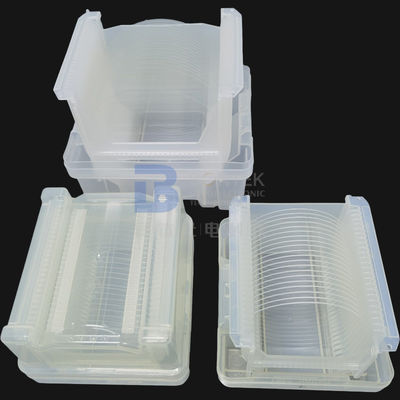
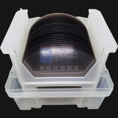
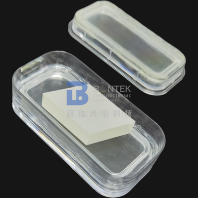
| Packaging Details: | Cassette/ Jar package, vaccum sealed |
| Delivery Time: | 1-4 weeks |
| Payment Terms: | T/T |
| Supply Ability: | 50000 pcs/Month |
|
Detail Information |
|||
| Product Name: | Piezoelectric Wafer | Diameter: | 3'', 4'', 6'', 8'' |
|---|---|---|---|
| Crystal Material: | LiTaO3, LiNbO3, Quartz | Thickness: | 0.35mm, 0.5mm, 1mm |
| Primary Flat: | 32.5±2mm, 47.5±2mm, 57.5±2mm | Cleaness: | Class 1000 |
| Application: | Semiconductor, Piezoelectric Devices | Inspection Report: | TTV, BOW, Warp, Ra |
| Highlight: | 8'' piezoelectric crystal wafer,6'' semiconductor wafer,4'' piezoelectric crystal wafer |
||
Product Description
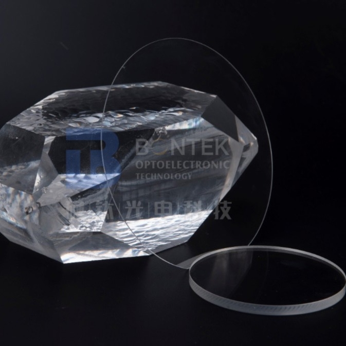
Semiconductor Cleaned Piezoelectric Wafer in stock in Class 1000 Clean Room
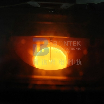
The piezoelectric effect in a crystal is explained as that there will be the development of electric charges on the metal surfaces when certain pressure or stress is applied to the piezoelectric crystal. This effect is reversible which means that the result will be electrical deformations in the material upon the application of the electric field. This is called a reverse piezoelectric effect.
BonTek grows crystal and fabricate wafers, we are piezoelectric specialist. Specially, we are capable of fabricating these materials into LARGE and THIN wafers. 3" 4" 6" 8" are all available as per requirement. In addition, we possess Corning Flatmaster 200 Profiler, Laser marking equipment, AOI and 6-step cleaning line.
![]()
![]()
![]()
|
Crystal |
LiNbO3 | LiTaO3 | SiO2 Crystal |
|
Diameter |
3’’, 4’’, 6’’, 8’’ | 3’’, 4’’, 6’’ | 3’’, 4’’, 5’’, 6’’, 8’’ |
|
Orientation |
X / Y / Y41 / Y64/Y128 |
X / X112 / YZ Y28 / Y36 / Y42 |
X / Y / Z AT36 / ST42.75 |
|
Surface Finish |
Single side polish / Double side polish | ||
|
Thickness |
0.08mm / 0.25mm / 0.35mm / 0.50mm / 1.00mm / 2.00mm | ||
|
LTV |
< 1.5um | ||
|
PLTV |
>98% (5mm*5mm) | ||
|
TTV |
< 5um | ||
|
Bow |
-25um < bow < +25um | ||
|
Warp |
< 35um | ||
|
Curie Temperature |
1142℃ ± 2℃ | 605℃ ± 2℃ | 573℃ |
|
Edge Profile |
CompI’t with SEMI M1.2 @ with GC#1000 | ||
|
Orientation Flat |
22±2mm, 32.5±2mm, 47.5±2mm, 57.5±2mm, Notch As per request |
||
|
Dope |
Er, MgO | Fe | with or without seed |
|
Front Side |
Roughness Ra<= 10A | ||
|
Back Criteria |
Roughness Ra: 0.5--1.0um GC#1000 | ||
|
Contamination |
Particles @ >0.3 micron | ||
|
Appearance |
No Cracks, saw marks, stains | ||
|
Single Domian |
Completed Polarization / Reduced | No Stress | |
![]()
![]()
FAQs:
- Q: What are the products you mainly work on?
A: We look at ourselves as the piezo wafer specialist. We are the very first to work with Single Crystal Quartz in China about 30 years ago. Then gradually we step in the field of LiNbO3, LiTaO3, Quartz glass, LGS, CTGS etc. Especially, if you are looking for a piezo quartz supplier, we are the ultimate choice! We export millions of quartz blanks each year because we master the AT, SC and IT cuts with superior angle precision.
- Q: Can you accept product customization?
A: Yes, of course. We can fabricate as per your request. In addition, we are so experienced with piezo wafers that we can provide you relevant suggestions if you are not 100% sure about your choice. Besides, we do have some standard wafers in stock, please check with us.
- Q: Can you deliver the goods via our courier agent?
A: Yes, we would suggest you go with the courier agent you are most familiar with (DHL, FedEX, UPS etc.). We can ship via your account. And, of course, we will pack the products safely in acceptable size to help you save the shipping cost. If you need us to take care of the freight, it’s also not a problem. We also have good discount with the international courier companies.
- Q: How can you guarantee we get what we want safely?
A: The wafer products are fragile and sometimes expensive. The last thing, as the manufacturer, we want to see is the products we make were damaged during courier. As a result, we will pack the wafers adequately and put them in a proper carton filled with buffer sponge. However, accidents are inevitable sometimes. So, please follow the “Acceptance check” steps shown in the drawings below. If the unwanted happened, we will either give the replenishment or refund if you follow the checking steps.
- Q: Can we visit your factory?
A: Sure. Factory inspection is important for large quantity purchase and long-term cooperation. Face to face discussion is what we mostly confident with. During the past years, big names around the world have witnessed our progress in factory build-up. These days, due to the Covid-19 pandemic, we also had the experience of videoconferencing with global buyers.
Acceptance Check
![]()
- The product is fragile. We have adequately packed it and labeled it fragile. We deliver through excellent domestic and international express companies to ensure transportation quality.
- After receiving the goods, please handle with care and check whether the outer carton is in good condition. Carefully open the outer carton and check whether the packing boxes are in alignment. Take a picture before you take them out.
- Please open the vacuum package in a clean room when the products are to be applied.
- If the products are found damaged during courier, please take a picture or record a video immediately. DO NOT take the damaged products out of the packaging box! Contact us immediately and we will solve the problem well.