100um Single Crystal Quartz Wafer For SAW Filter Piezo Oscillator Resonator Accelerator
Product Details:
| Place of Origin: | China |
| Brand Name: | BonTek |
| Certification: | ISO:9001, ISO:14001 |
| Model Number: | Piezoelectric Wafer |
Payment & Shipping Terms:
| Minimum Order Quantity: | 5 pcs |
|---|---|
| Price: | Negotiable |
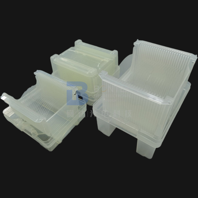
| Packaging Details: | Cassette/ Jar package, vaccum sealed |
| Delivery Time: | 1-4 weeks |
| Payment Terms: | T/T |
| Supply Ability: | 50000 pcs/Month |
|
Detail Information |
|||
| Name: | Piezoelectric Wafer | Diam.: | 3 Inch, 4 Inch, 6 Inch |
|---|---|---|---|
| Material: | Alpha Quartz | Thickness: | 100um Up |
| Flat: | 22mm, 32.5mm, 47.5mm, 57.5mm, Notch | Surface Finish: | Double Side Polish, Single Side Polish |
| Use: | Surface Acoustic Wave Application | Ra: | <1nm, <0.5nm |
| Highlight: | Crystal Quartz Piezoelectric Wafer,SAW Filter Single Crystal Quartz Wafer,Piezo Single Crystal Quartz Wafer |
||
Product Description
Single Crystal Quartz Wafer For SAW Filter Piezo Oscillator Resonator Accelerator
The cutting of quartz wafer to a certain orientation of the crystal coordinate axis is called the cutting pattern of quartz wafer. Due to the anisotropy of quartz crystal, the electrical and thermal properties of quartz slices are different due to their different elastic properties, piezoelectric properties and temperature properties.
There are two ways to express the cut symbol of quartz crystal, one is the symbol representation prescribed by IRE standard, the other is the custom symbol representation peculiar to quartz crystal. IRE (cut type prescribed by the symbol (XYZlWt) with a set of letters and Angle, said with XYZ three letters in order to represent the chip thickness and length along the axis of the original location, with t (thickness), l (length), W (width) to represent the rotating direction, Angle counterclockwise said plus and minus sign said clockwise.
![]()
![]()
![]()
|
Material |
Synthetic Piezoelectric Quartz Crystal |
|||
|
Cutting Angle |
X / Y / Z / AT32°/33°/35°/36°/ BT / ST42.75° etc. or per Customized |
|||
|
Diameter/size |
3" (76.2mm) |
4" (100mm) |
6" (150mm) |
8" (200mm) |
|
Tol(±) |
<0.20 mm |
|||
|
Thinnest Thickness |
0.08mm Min-up |
0.10mm Min-up |
0.20mm Min -up |
0.35mm Min- |
|
Primary Flat |
22mm |
32mm |
42.5mm |
57.5mm or notch |
|
LTV (5mmx5mm) |
<1.5µm |
|||
|
TTV |
<1.5~10 µm |
|||
|
Bow |
±10~±50um |
|||
|
Warp |
<10~40µm |
|||
|
PLTV(<0.5um) |
≥95%(5mm*5mm) |
|||
|
Orientation Flat |
All available |
|||
|
Surface Type |
Single Side Polish / Double Side Polish / Lapped |
|||
|
Polished side Ra |
<0.5nm or specific per requested |
|||
|
Back Side Criteria |
General is 0.2-0.5µm or as customized |
|||
|
Edge Criteria |
R=0.2mm or Bullnose |
|||
|
Material Property |
ECD |
Better than grade 4 |
||
|
Inclusion |
Better than grade II |
|||
|
Q-Value |
Better than grade C |
|||
|
Wafer Surface Criteria |
Particles ¢>0.3 µ m |
<= 30 |
||
|
Scratch, Chipping |
None |
|||
|
Defect |
No edge cracks, scratches, saw marks, stains |
|||
|
Packaging |
Qty/Wafer box |
25pcs per box, Semi Standard |
||
![]()
![]()
Acceptance Check
![]()
- The product is fragile. We have adequately packed it and labeled it fragile. We deliver through excellent domestic and international express companies to ensure transportation quality.
- After receiving the goods, please handle with care and check whether the outer carton is in good condition. Carefully open the outer carton and check whether the packing boxes are in alignment. Take a picture before you take them out.
- Please open the vacuum package in a clean room when the products are to be applied.
- If the products are found damaged during courier, please take a picture or record a video immediately. DO NOT take the damaged products out of the packaging box! Contact us immediately and we will solve the problem well.


