


 |
Sapphire Windows Piezoelectric Wafer Semiconductor Scratching Resistant
Product Details:
| Place of Origin: | China |
| Brand Name: | BonTek |
| Certification: | ISO:9001 |
| Model Number: | Sapphire (Al2O3) |
Payment & Shipping Terms:
| Minimum Order Quantity: | 5 Pieces |
|---|---|
| Price: | Negotiable |
| Packaging Details: | Cassette, Jar, Film package |
| Delivery Time: | 1-4 weeks |
| Payment Terms: | T/T |
| Supply Ability: | 10000 pieces/Month |
|
Detail Information |
|||
| Material: | Sapphire Windows | Growth: | Kyropoulos Method |
|---|---|---|---|
| Melting Point: | 2040 °C | Thermal Conductivity: | 27.21 W/(m X K) At 300 K |
| Thermal Expansion: | 5.6 X 10 -6 /K (parallel C-axis) & 5.0 (perpendicular C-axis) X 10 -6 /K | Hardness: | Knoop 2000 Kg/mm 2 With 2000g Indenter |
| Specific Heat Capacity: | 419 J/(kg X K) | Dielectric Constant: | 11.5 (parallel C-axis) 9.4 (perpendicular C-axis) At 1MHz |
| Highlight: | Semiconductor Piezoelectric Wafer,Sapphire Windows Piezoelectric Wafer,Scratching Resistant Sapphire Wafer |
||
Product Description
Semiconductor Sapphire Wafer Sapphire Windows Piezoelectric Wafer
Sapphire is a material of a unique combination of physical, chemical and optical properties, which make it resistant to high temperature, thermal shock, water and sand erosion, and scratching. It is a superior window material for many IR applications from 3µm to 5µm. C-plane sapphire substrates are widely used to grow III-V and II-VI compounds such as GaN for blue LED and laser diodes, while R-plane sapphire substrates are used for the hetero-epitaxial deposition of silicon for microelectronic IC applications.
![]()
![]()
![]()
|
Item |
3-inch C-plane(0001) 500μm Sapphire Wafers |
|
|
Crystal Materials |
99,999%, High Purity, Monocrystalline Al2O3 |
|
|
Grade |
Prime, Epi-Ready |
|
|
Surface Orientation |
C-plane(0001) |
|
|
C-plane off-angle toward M-axis 0.2 +/- 0.1° |
||
|
Diameter |
76.2 mm +/- 0.1 mm |
|
|
Thickness |
500 μm +/- 25 μm |
|
|
Primary Flat Orientation |
A-plane(11-20) +/- 0.2° |
|
|
Primary Flat Length |
22.0 mm +/- 1.0 mm |
|
|
Single Side Polished |
Front Surface |
Epi-polished, Ra < 0.2 nm (by AFM) |
|
(SSP) |
Back Surface |
Fine ground, Ra = 0.8 μm to 1.2 μm |
|
Double Side Polished |
Front Surface |
Epi-polished, Ra < 0.2 nm (by AFM) |
|
(DSP) |
Back Surface |
Epi-polished, Ra < 0.2 nm (by AFM) |
|
TTV |
< 15 μm |
|
|
BOW |
< 15 μm |
|
|
WARP |
< 15 μm |
|
|
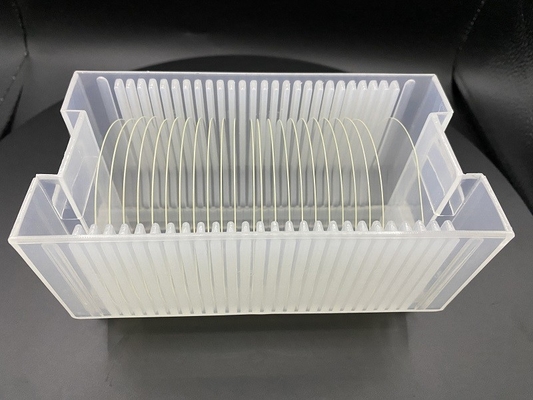
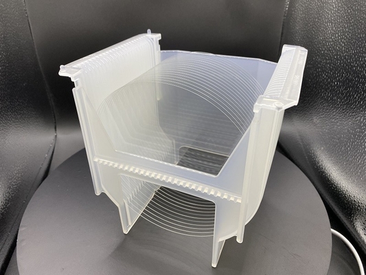
Cleaning / Packaging |
Class 100 cleanroom cleaning and vacuum packaging, |
|
|
25 pieces in one cassette packaging or single piece packaging. |
||
|
Item |
4-inch C-plane(0001) 650μm Sapphire Wafers |
|
|
Crystal Materials |
99,999%, High Purity, Monocrystalline Al2O3 |
|
|
Grade |
Prime, Epi-Ready |
|
|
Surface Orientation |
C-plane(0001) |
|
|
C-plane off-angle toward M-axis 0.2 +/- 0.1° |
||
|
Diameter |
100.0 mm +/- 0.1 mm |
|
|
Thickness |
650 μm +/- 25 μm |
|
|
Primary Flat Orientation |
A-plane(11-20) +/- 0.2° |
|
|
Primary Flat Length |
30.0 mm +/- 1.0 mm |
|
|
Single Side Polished |
Front Surface |
Epi-polished, Ra < 0.2 nm (by AFM) |
|
(SSP) |
Back Surface |
Fine ground, Ra = 0.8 μm to 1.2 μm |
|
Double Side Polished |
Front Surface |
Epi-polished, Ra < 0.2 nm (by AFM) |
|
(DSP) |
Back Surface |
Epi-polished, Ra < 0.2 nm (by AFM) |
|
TTV |
< 20 μm |
|
|
BOW |
< 20 μm |
|
|
WARP |
< 20 μm |
|
|
Cleaning / Packaging |
Class 100 cleanroom cleaning and vacuum packaging, |
|
|
25 pieces in one cassette packaging or single piece packaging. |
||
|
Item |
6-inch C-plane(0001) 1300μm Sapphire Wafers |
|
|
Crystal Materials |
99,999%, High Purity, Monocrystalline Al2O3 |
|
|
Grade |
Prime, Epi-Ready |
|
|
Surface Orientation |
C-plane(0001) |
|
|
C-plane off-angle toward M-axis 0.2 +/- 0.1° |
||
|
Diameter |
150.0 mm +/- 0.2 mm |
|
|
Thickness |
1300 μm +/- 25 μm |
|
|
Primary Flat Orientation |
A-plane(11-20) +/- 0.2° |
|
|
Primary Flat Length |
47.0 mm +/- 1.0 mm |
|
|
Single Side Polished |
Front Surface |
Epi-polished, Ra < 0.2 nm (by AFM) |
|
(SSP) |
Back Surface |
Fine ground, Ra = 0.8 μm to 1.2 μm |
|
Double Side Polished |
Front Surface |
Epi-polished, Ra < 0.2 nm (by AFM) |
|
(DSP) |
Back Surface |
Epi-polished, Ra < 0.2 nm (by AFM) |
|
TTV |
< 25 μm |
|
|
BOW |
< 25 μm |
|
|
WARP |
< 25 μm |
|
|
Cleaning / Packaging |
Class 100 cleanroom cleaning and vacuum packaging, |
|
|
25 pieces in one cassette packaging or single piece packaging. |
||
![]()
Acceptance Check
![]()