


 |
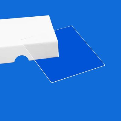
Precision Cut Sapphire Wafer Al2O3 Crystal Substrate Providing Superior Durability And Thermal Conductivity For Devices
Product Details:
| Place of Origin: | China |
| Brand Name: | CQT |
| Certification: | ISO:9001 |
| Model Number: | Sapphire (Al2O3) |
Payment & Shipping Terms:
| Minimum Order Quantity: | 10 Pieces |
|---|---|
| Price: | Negotiable |
| Packaging Details: | Cassette, Jar, Film package |
| Delivery Time: | 1-4 weeks |
| Payment Terms: | T/T |
| Supply Ability: | 10000 pieces/Month |
|
Detail Information |
|||
| Material: | Sapphire (Al2O3) Crystal | Type: | Single Crystal |
|---|---|---|---|
| Color: | White / Red / Blue | Diameter: | 2" 3" 4" 6" |
| Growth Method: | Horizontally Directed Crystallization (HDC) | Surface: | DSP SSP |
| Shear Modulus (G): | 148.1 GPa | Industry: | Led,optical Glass,eli-ready Wafer |
| Highlight: | Precision cut sapphire wafer substrate,Al2O3 crystal substrate for devices,Durable piezoelectric wafer with thermal conductivity |
||
Product Description
Precision Cut Sapphire Wafer Al2O3 Crystal Substrate Providing Superior Durability And Thermal Conductivity For Devices
For industries demanding exceptional durability, thermal stability, and optical clarity, our Sapphire Wafers are engineered to deliver unmatched precision and reliability. Crafted from single-crystal sapphire (α-Al₂O₃), these wafers excel in high-stress environments, including LED manufacturing, semiconductor substrates, optoelectronics, and aerospace applications.
Renowned for their ultra-high hardness (Mohs 9), sapphire wafers resist scratches, wear, and chemical corrosion, ensuring long-term performance in harsh conditions. Their outstanding thermal conductivity (35 W/m·K) and low thermal expansion coefficient minimize distortion during rapid temperature changes, making them ideal for high-power electronics and laser systems. Additionally, sapphire’s broad optical transparency (from UV to near-IR) supports advanced imaging and sensor technologies.
Available in custom diameters, thicknesses, and orientations (e.g., C-plane, R-plane), our wafers meet stringent industry standards for flatness, surface roughness, and purity. Whether used as protective windows, substrate materials, or acoustic devices, our Sapphire Wafers provide a cost-effective, high-performance solution.
Elevate your applications with the ultimate in strength and clarity—choose our Sapphire Wafers for uncompromising quality. Contact us today to request a quote or discuss your project needs!
![]()
![]()
![]()
OPTICAL PROPERTIES
|
Transmission |
0.17 to 5.5 um |
|
Refractive Index |
1.75449 (o) 1.74663 (e) at 1.06 um |
|
Reflection Loss |
at 1.06 microns (2 surfaces) for o-ray - 11.7%; for e-ray - 14.2% |
|
Absorption Index |
0.3 x 10⁻³ cm-1 at 2.4 um |
|
dN/dT |
13.7 x 10⁻⁶ at 5.4 um |
|
dn/dm = 0 |
1.5 um |
|
Orientation |
R-plane, C-plane, A-plane, M-plane or a specified orientation |
|
Orientation Tolerance |
± 0.3° |
|
Diameter |
2 inches, 3 inches, 4 inches, 6 inches, 8 inches or others |
|
Diameter Tolerance |
0.1mm for 2 inches, 0.2mm for 3 inches, 0.3mm for 4 inches, 0.5mm for 6 inches |
|
Thickness |
0.25mm, 0.33mm, 0.43mm, 0.65mm, 1mm or others; |
|
Thickness Tolerance |
25μm |
|
Primary Flat Length |
16.0±1.0mm for 2 inches, 22.0±1.0mm for 3 inches, 30.0±1.5mm for 4 inches, 47.5/50.0±2.0mm for 6 inches |
|
Primary Flat Orientation |
A-plane (1 1-2 0 ) ± 0.2°; C-plane (0 0-0 1 ) ± 0.2°, Projected C-Axis 45 +/- 2° |
|
TTV |
≤10µm for 2 inches, ≤15µm for 3 inches, ≤20µm for 4 inches, ≤25µm for 6 inches |
|
BOW |
≤10µm for 2 inches, ≤15µm for 3 inches, ≤20µm for 4 inches, ≤25µm for 6 inches |
|
Front Surface |
Epi-Polished (Ra< 0.3nm for C-plane, 0.5nm for other orientations) |
|
Back Surface |
Fine ground (Ra=0.6μm~1.4μm) or Epi-polished |
|
Packaging |
Packaged in a class 100 clean room environment |
![]()
Acceptance Check
![]()
1. The product is fragile. We have adequately packed it and labeled it fragile. We deliver through excellent domestic and international express companies to ensure transportation quality.
2. After receiving the goods, please handle with care and check whether the outer carton is in good condition. Carefully open the outer carton and check whether the packing boxes are in alignment. Take a picture before you take them out.
3. Please open the vacuum package in a clean room when the products are to be applied.
4. If the products are found damaged during courier, please take a picture or record a video immediately. DO NOT take the damaged products out of the packaging box! Contact us immediately and we will solve the problem well.